![]()
|
|
Personal web pages ofTim Stinchcombe |
Plan B M32 Vector Plotter modificationsWhen I originally reverse-engineered one of these modules I couldn't be bothered to work out how to correct its many flaws, as there aren't that many of them out there: one post at the old Plan B Yahoo group stated that they had bought just 100 joysticks, whilst another (in the middle of the Plan B collapse) proclaimed that 'all 50 have been built', so it is very likely the actual number of them is 100 or less, and possibly even just as few as 50. However, having expended some effort repairing a badly burnt-up one, it seemed pointless not to carry on and rectify the other issues the module has, but due to the low numbers involved some detail may be brief. Revisions: earlier versions are marked 'rev 1.0' in the silkscreen on both boards, and are plastered with cuts, straps and factory-fitted mods compared to later 'rev 1.1' revisions (I count about 13 cuts, 5 sets of straps and 3 resistor/trimpot mods). Most of these mods were incorporated properly into the PCB design at rev 1.1, but a couple of new ones crept in, and it looks like one crucial track cut had not been detected in rev 1.0 (identified in the next section).
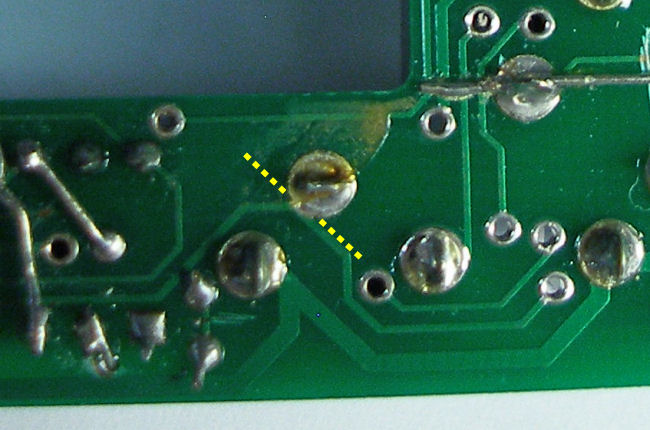
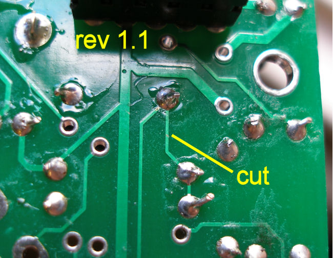
A warning: on the rev 1.0 version the silkscreen outlines for ICs U2, U3 and U4 are reversed, so if you remove these chips to work on the module, make sure you don't replace them as the silkscreen indicates, or they will be reversed (and then maybe ...poof...!). The blow-up on the module I repaired was caused by an undetected DRC failure ('design rule check'): a track too close to a pad, so they were shorting. That my rev 1.1 does have a cut to remove this short strongly suggests this fault was not detected until after modules were shipped with it, rather than it being a factory mod that was missed. It is under the 'X/Y KIN GATE' socket on the jack board, and requires a cut with a sharp knife to isolate the pad from the track, in the direction highlighted:
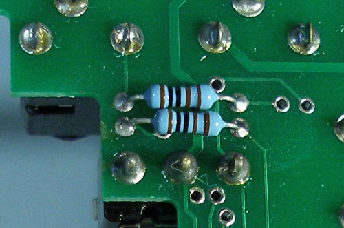
The fault sticks −12V onto one of the AND gate outputs of the 4081 quad AND gate chip, which eventually blows (a matter of minutes apparently!); the 200Ω resistor on the output was also badly burnt; and the Z-gate transistor was also damaged and so also needed replacing (it is connected to another 4081 input, and is the only transistor in the design). The following is the location of the gate output resistors on the rev 1.0 jack board, near the 'positive/bipolar' switch (taken after a precautionary increase to 1kΩ and 0.6 watt types, before I had identified the real cause of the problem, the short):
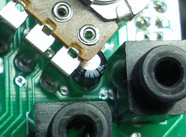
(Rev 1.1 units shouldn't have this issue, as the cut should have been made as one of the factory-fitted mods; in rev 1.1 the output resistors got moved to the top of the board, in amongst the jacks, so aren't as conspicuous as on the rev 1.0.) Precautionary reversal of electrolytic cap on −12V rail: this cap, shown in the correct orientation, tucked in between the X-axis LEVEL pot/KINETIC GATE jack/D EXT IN jack, is likely to have been inserted the wrong way when built, as the silkscreen orientation is wrong (so replace it, or turn it around, which will likely be OK as long as it still measures close to what it should be, 10μF):
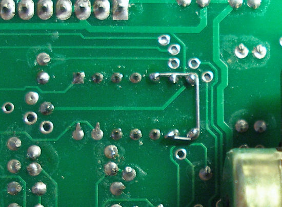
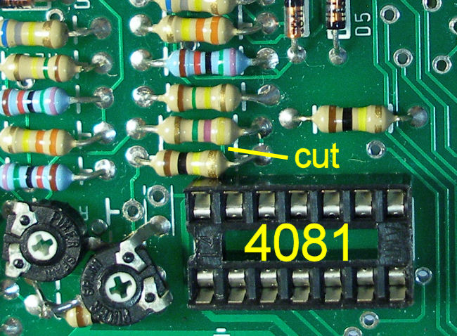
Ground unused CMOS inputs: two of the gates in the 4081 quad AND gate chip (I can't see a 'Ux' identifier for it) are left floating. Whilst there is no evidence that this in itself is causing any particular problem, it is bad practice, and since it is easy to correct it would seem foolish not to do so given how much else needs doing. Running a strap around pins 5, 6, 7 (ground), 8 and 9 will do it (rev 1.0 shown—tracking on the rev 1.1 looks a little different—and this photo was taken before the other mods below were installed):
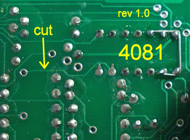
Abuse of CMOS inputs: (note that performing this mod mandates doing the multiple resistor changes below, otherwise the comparators may not switch properly). The X and Y kinetic gates are produced by op amps wired as comparators; these are fed directly into the inputs of one of the AND gate sections in the 4081 in order to combine them; thus when the op amps attempt to swing down to the negative rail, the input protection diodes in the 4081 clamp the outputs to a diode-drop below ground, and dump all the current the op amps can take; this makes both the op amps and the 4081 run rather hot (the op amps are spec'd to take this, but who knows what the longer-term affects on the 4081 will be...). Cutting a couple of tracks and adding diodes and resistors prevents this from happening (performing this mod more than halves the module's current draw, from around 130mA down to 55mA or so). Doing the mod requires two 1N4148 diodes, two 10kΩ resistors, and cutting two tracks. Locate this track under the 4.7MΩ resistor—it runs from the left end of the resistor to pin 12 on the 4081. There is just about room between the resistors to cut the track:
The other track to cut, running to pin 13 of the 4081, is easily identifiable under the board:
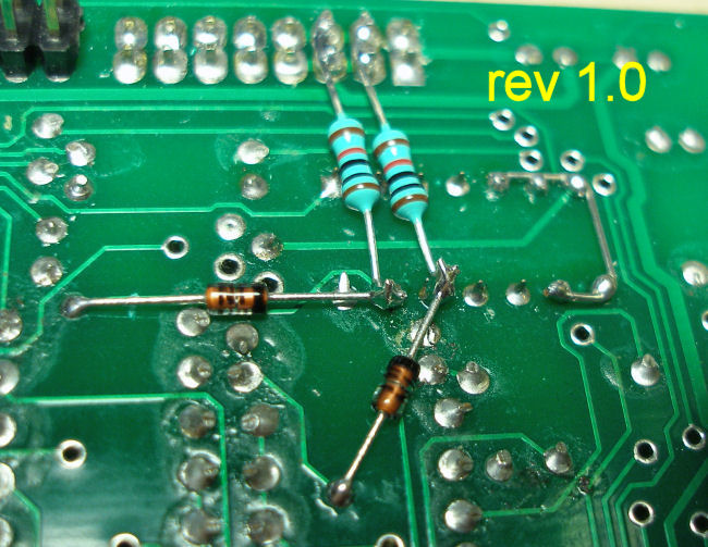
Then solder the 10kΩ resistors from pins 12 and 13 to ground (the power connector is handily nearby), and the diodes (cathodes toward the 4081 pins) from the vias shown (and of course, make sure that the leads do not make contact with any other pins nearby!):
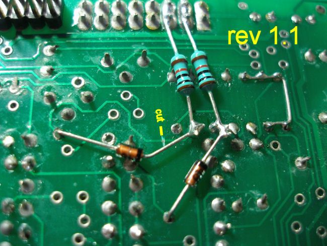
The tracking for the rev 1.1 board is ever so slightly different (and which meant I routed the one diode slightly differently, to avoid stuff; I also made the track cut closer to pin 13):
In addition, a fault was introduced on the jack board in going to rev 1.1, which inadvertently shorted a diode out, and it is important to cut this in order that the negative swing of the X kinetic gate output doesn't go down to the negative rail (before doing the mod, the abused 4081 input was preventing this!):
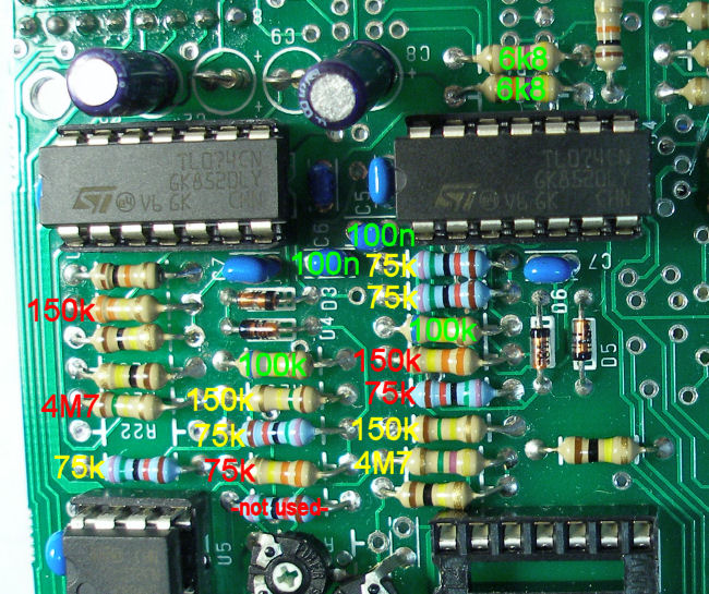
Kinetic gate re-scaling. The kinetic gates are implemented by a differentiator detecting the rate of change of the stick movement; followed by full-wave rectifiers (so falling and rising slopes always produce a positive voltage); then comparators with adjustable levels (to be able to alter the 'sensitivity') trigger/don't trigger appropriately. I really couldn't get much sense out of mine at all: it sort of worked on the one axis, but I got little out of the other. There were four resistor locations different between the two axes, though I would have expected them to be identical, and even within each side the values installed in the rectifiers didn't give proper rectification. Hence a complete re-vamp seemed called for. With the existing values I found the differentiator to be saturating at too-low a rate; it was also so noisy at higher frequencies it was impossible to get anything like a constant voltage out given a steadily rising or falling waveform input (a common problem for differentiators, though in fairness to the original design there is substantial lowpass filtering in the rectifiers, but it meant it was very difficult to see what the differentiator was doing). The mismatched resistors in the rectifiers meant positive and negative swings had different gains (see graph below); the comparators also weren't symmetric across X and Y either. The following annotated photo shows suggested values which make all of these things better: the trimpots can then be adjusted over a fairly wide range in order to set the kinetic gate to trigger for slow or fast movements of the joystick. The green values are for the differentiators, and will need changing: two 47kΩ resistors above U4 become 6.8kΩ; two 680kΩ resistors reduce to 100kΩ; and the caps C5 and C6 leap from 22pF ('22') up to 100nF. Yellow values are most likely already correct (but check!). Red values will most likely need changing, but there were differences between the rev 1.0 and 1.1 units I've seen:
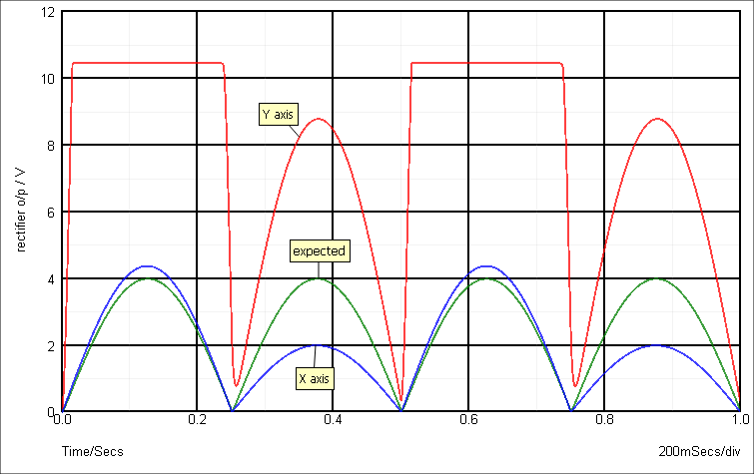
Trimpots: the one nearest U5 is for the X-axis; the other one (nearer the 4081 chip) is for the Y-axis. Adjust clockwise to make the gate more sensitive, i.e. a gentle movement will trigger it, and anticlockwise to make it harder to trigger, i.e. a much more aggressive movement is needed to trigger it (and note the gate won't work with the trimpot at either extremity, so back it off a bit!). On a slightly more technical level, here is simulation output of the X and Y rectifier sections, showing the asymmetric performance due to the mish-mash of resistor values fitted (the input being a ±4V sinewave):
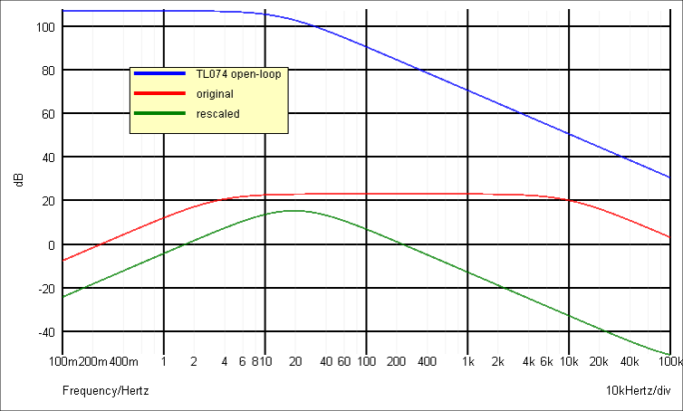
And here is the response of the differentiator, in its original form (red), and what my re-scaling makes it (green):
Moving the upward high-pass 's' slope right allows slightly faster rates to be distinguished by the differentiator, and bringing the second pole right down (by the 22p to 100n cap change) means that we get a low-pass effect as soon as we pass the point where we don't need any more differentiation action, thus knocking the high-frequency noise on the head. (I thought the cap change might be a bit much, but 100n is a nice convenient value, and its visible effect on transient waveforms didn't seem to be too much of an issue when compared to smaller values.) [Page last updated: 29 May 2019] |