![]()
|
|
Personal web pages ofTim Stinchcombe |
Plan B M15 VCO other modificationsThis page contains some simple modifications (swapping out components etc.) to the M15 VCO, mainly to bring earlier Rev 1 versions into line with later revisions of the module.
M15 module revision summary The M15 has been through four major physical (form factor) revisions; there were several electrical revisions, as circuitry was added or modified to improve or enhance performance; and there are numerous component fitment differences (basically different resistor values), again to achieve changes in performance. Unfortunately configuration control was clearly never one of Plan B's strong suits, as several of their modules exhibit PCBs which are functionally different in some way, but which bear the same revision level in the silkscreen printing on the PCB—the M15 is victim to this too. In some circumstances this can (understandably) make conversations or exchanges about the M15 difficult: the table attempts to summarize the functional differences between the different revision levels; the different physical configurations are thankfully easy to distinguish, and are described after the table. Here is a summary of the revision levels, and what changed etc., as best as I can tell. To be able to distinguish between the different form factors, I have 'adopted' a naming convention of sorts (I've little idea what method Plan B themselves may have used). (Superscripts refer to notes tucked-away at the bottom of the page, which back up some of the assertions):
M15 different form factors Rev 1: the initial release of the module had the main PCB perpendicular to the faceplate—it is about 4 inches deep, and rather vulnerable. The example shown doesn't have a rev level on the PCB, only a 'Copyright 2004' legend. The daughter board mounted on the main PCB is the exponential converter, and I assume the whole reason for making it separate was to allow it to be epoxy-sealed, but I have no knowledge that this was ever done—its circuitry was incorporated directly into the main PCB at rev 1.2. Rev 1.x levels went to 1.5—whether all the lower levels were actually released I don't know:
Rev 2.x: the first major revision had the main PCB moved to be parallel to the faceplate and attached to it via three smaller PCBs, perpendicular to both the faceplate and the main PCB and which hold the majority of the jack sockets and potentiometers. I have seen versions with the main PCB marked '2.1' and '2.4'—whether versions 2.2 and 2.3 were actually released or not I don't know. I suspect this will be the most numerous version built of the three configurations:
Rev 2.5: the second major revision dispensed with the three perpendicular boards, and consists of two PCBs parallel to the faceplate: the outer one houses the majority of components; the inner one holds vertical-mount jacks and the potentiometers (the photos don't have the faceplate on, obviously!) (This is a 2.4/2.5, as the vactrol is on the back of the main board, just visible at bottom-left of the top photo):
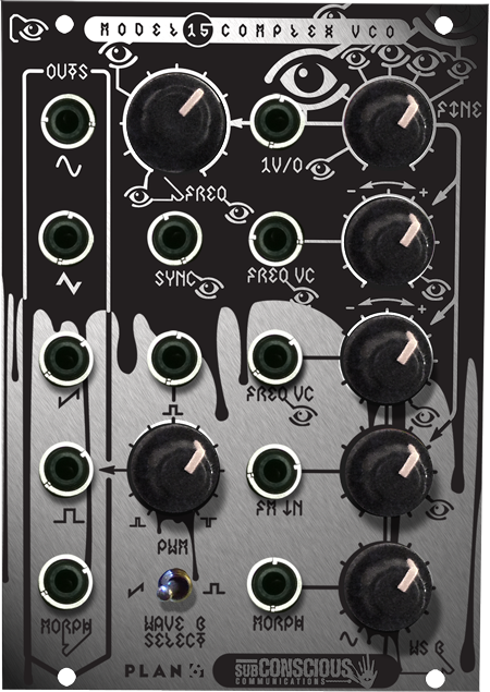
Subcon: in late 2011/early 2012 Subconscious Communications did a limited run of 110 modules in yet a fourth form factor revision. The most obvious distinguishing characteristic is the strikingly-different faceplate from the Plan B version:
The module is much shallower than previous revisions, due to its other defining characteristic—the PCB has been re-laid out using surface-mount devices, thus drastically reducing the total amount of PCB area required:
If the PWM pot on your M15 looks something like this:
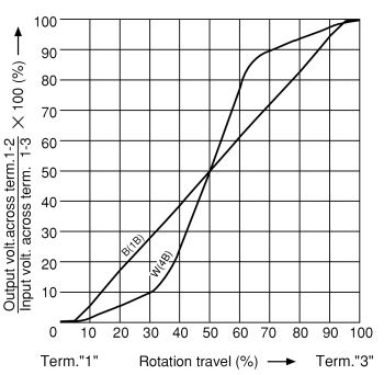
the 'W' of the 'W100K' being the notable bit, then there is a good chance that you find the range over which the pot actually has an effect on the waveform to be rather restrictive! Fortunately the means to improve it considerably is simple—replace the pot with a 'B100K' type instead! (I suspect these pots may be fitted to modules at all revision levels.) There is some impact on the issue from the resistor-value choices in the circuit (about 5 or 6 of them), but it is largely caused by the choice of the 'W' taper for the pot. The following plot (culled from an Alps datasheet) shows how the 'W' taper has a near 'S' shape to it, where the steeper slope of the centre section means that you get a much greater change in wiper voltage for the same amount of pot travel:
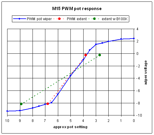
In the circuit, the amount of PWM is determined by the voltage at the pot wiper, and so having the voltage change quickly for small changes in pot position (compared to the more familiar 'B' taper) means that the PWM is harder control and operates over a much reduced range of pot travel. Here is a plot of the pot wiper voltage against the (rough) pot position (solid blue trace), confirming the shape of the W taper from an actual module (the x-axis is reversed so it compares to the ideal above; the wiper voltage has an offset due to the requirements of the circuit):
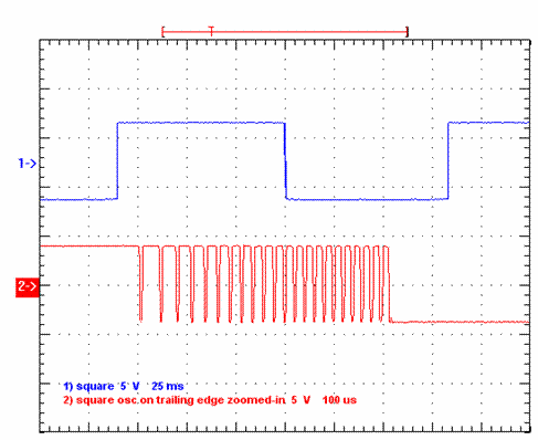
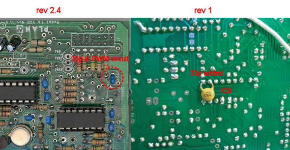
The red broken line shows the extent that the PWM is effective over—outside of this region the square wave is 'extinguished' because it goes to one rail or the other, and so is inaudible—and we see that this occupies only about the middle third of the pot travel. Simply replacing the pot with a standard 'B' linear taper-type shows that more pot travel is required to change the voltage, and hence the PWM is effective over a larger amount of pot travel, the green broken line, with perhaps more like two-thirds of the pot travel being usable now. (Here is the Plan B M15 PWM pot response thread at ModWiggler where this was initially discussed.) Oscillation on square wave trailing edge (early revisions only): this arises due to unwanted capacitive coupling between the 'square out' traces/wiring, and the 'PWM CV in' traces/wiring, and it is readily removed by adding a capacitor that appears in later revisions of the circuit. The problem manifests itself as an oscillation, or 'indecision to switch', on the trailing edge (i.e. high to low transition) of the square wave output, and it is only present at lower frequencies, below about 480-500Hz (traces are from an early Rev 1 module; susceptibility to the oscillation appears to depend on the type of chip fitted too—TL084s seem more likely to oscillate than TL074s):
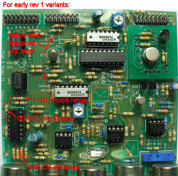
Morph changes (Rev 1) It seems Plan B did quite a lot of experimentation—chopping and changing of resistor values—before the performance of the morph circuit was even half-way decent in later revisions of the module (and which still leaves room for improvement). The following photo shows what to change on an early Rev 1 PCB in order to bring it more in line with later revisions—sections following the photo explain what the impact of each change is (and it is quite possible that later Rev 1 revisions may have different component fitments...):
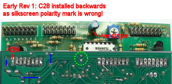
Overall morph amplitude: the change '0Ω link: overall ampl' is to replace the 100kΩ resistor with a short (this brings it in line with at least revs 2.4 and 2.5, and perhaps earlier). The 100kΩ, with the 82kΩ below it, gives a gain of just under two for the morph circuit, which makes the sine in particular have a rather large swing—with the short, the buffer is simply a unity gain one, making the sine about ±5V, the saw ±3.5V, and with the 'square wave amplitude' mod below, the square about ±3V. Morph range: with the original 10kΩ resistor at this location, the actual morphing action takes place in a very narrow range of pot travel and/or morph CV voltage. Replacing it with a 1.2kΩ, the value used in Rev 2.4, means the morph between the sine and saw/square takes place over a much wider range, making the transition much less abrupt. (In the Rev 2.4/2.5 there is a an even lower value at this location, 220Ω, but I haven't tried this to see what effect it has in practice; apparently in the Rev 2.5/2.5 this resistor reverted back to a 1.2kΩ) Morph CV control range: the change '12k:CV ctrl range' is to swap the 22kΩ with a 12kΩ. With the 22kΩ, it takes about a 10V sweep at the CV input to perform a full morph from one waveform to the other; reducing the resistor to 12kΩ means that only about 5V is needed to do the full morph, a voltage range that is probably more easily realisable with typical Eurorack modules (an offset will need to be dialled in using the morph pot though). (This change can also be done to Revs 2.x and 2.5 too—see below.) Morph square wave amplitude: when switched through to the input of the morphing circuit, the square wave is taken directly from the comparator generating it from the tri wave, rather than the divided-down signal at the square output jack; the comparator signal swings nearly rail-to-rail, and thus when the morph becomes 'fully square', there is a huge increase in amplitude in comparison to the sine wave morphed from. This can be alleviated by moving the wire (which comes from the 'wave select' switch) from the hole marked 'SQR' and soldering it to the end of the 1kΩ resistor as shown ('Move wire: morphed sqr ampl'). The resulting square wave coming out of the morph circuit then swings about ±3V. (This assumes that the square output is divided-down—on the early Rev 1 version shown, this is achieved with a 680Ω resistor added directly to the square output jack, and it should be fairly obvious if it is not there, as then the square output itself will swing nearly rail-to-rail.) (This change can also be done to Revs 2.x and 2.5 too—see below.) Morph changes (Revs 2.x and 2.5) TBA Reversed polarised capacitor: (Rev 1) On the early rev 1 unit I worked on I noted that 10μF electrolytic capacitor C28 (bypassing the −12V rail) was installed backwards, most likely because the polarisation mark on the silkscreen is the wrong way round. It is easy to check with a simple continuity tester, by beeping through the blue lines (in reality 0Ω links) indicated, that the outermost trace is in fact the −12V rail, and thus the negative stripe on the capacitor should face outwards:
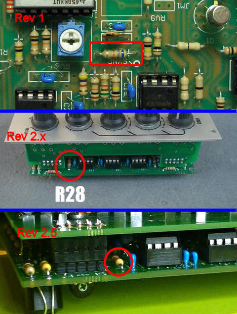
(The polarising '+' mark is on the pin nearest the edge of the board, and hard to capture photographically as it is right under the capacitor of course!) I have since received reliable information that indicates that this error occurs on all rev 1 levels—on later rev 1s, the capacitor is in the same place, but is designated as C14. This puts a lie to the notion that any reversed electrolytic will immediately explode—to prevent that from happening in the future though it ought to be replaced, or at the very least turned around (electrolytic caps can 'recover' to a certain extent). (It didn't carry over to the Rev 2 version due to the substantial re-working the main PCB underwent.) Hard sync modification (all rev levels) I'm really only providing this for completeness, as I haven't examined the action of lowering the resistor concerned, R28, in any great detail. However looking at the circuit, R28 determines the upper switching point of the comparator at the core of the oscillator, and lowering it will increase the amplitude of the triangle wave developed in the core—the sinewave is derived directly from this signal, and so it is quite likely that changing R28 will require some tweaking of the sinewave trimpots in order to reset that for minimal distortion. The sync input feeds directly through R28 to the comparator, and thus that input has a direct effect on the points where the oscillator switches, hence the syncing effect, and (very likely) why changing its value may have a sonically different/interesting effect (but as I say, I've not looked at the detail, nor even scoped it...).
It was originally suggested at the Plan B Yahoo group—here is the post, #927, Hard sync modification - Model 15, Apr 27, 2007: Just to show that I listen to ou guys, if you want to make your Model 15 sync from what it is stock to a very hard, change R28 (a 56K horizontally-positioned resistor right below the SYNC wire on the PCB to 10K. Another option is just floating a 12k over the 56K without removing it - so you solder the leads of the 12 to the leads of the 56K. Just make sure those leads don't touch anything else if you go that route. This is what it'l sound like: http://www.ear-group.net/hardsync.mp3 (I am also sweeping the frequency of the VCO you're listening to in this sample) I will shipping all new VCOs with this mod in. Judging by the fitments I've seen for this resistor, either I've seen build errors, or it is difficult to decide just what is best: The following photo shows the location of R28 across the different form factors/rev levels, should anyone feel inclined to 'dabble'!:
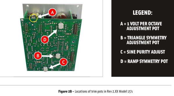
Notes and references from the revision summary table: gathered together here, for reference, are posts and photos backing up the assertions made in the revision summary table at the top of the page (placed at the bottom of the page merely to keep them out of the way; and text copied from the Yahoo group posts so non-members can read it): Note 1. Answer to the question: "Aside from the redesigned form factor and improved sine waveform, what are the differences between revision 1 and 2 Model 15 oscillators?" in post #1444 Re: Model 15 questions, Feb 17, 2008: The short answer is not much. Going into a little more detail, outside of a second change to the sine wave circuit (which was put there for easier initial set up (us) and really doesn't effect the end user and the 15A port, the differences are slight: We've added an output buffer to the PWM circuit (which was handled another way in the older versions) and a bypass cap or two. Nothing serious. The new (flat) VCO also has a pathway for the (I promise) soon to be released 15A expander. It's another connector. Look on this blog for what the 15A does. Btw - I've found the missing link which was making the +/- octave switch behave so poorly...so this should be coming out with the rest of the ELF's. Most the bigger changes had already happened by the time we flattened the unit out, namely: the AC offset triangle output (the first release was offset all above ground), the harmonically improved sine wave, the use of an SMT tempco resistor, the substitution of our analog switch - initially used only because I really thought I'd only be making 25 of these for that semi-custom , very limited order on the Doepfer list and I happened to have 150 of these really expensive 18 pin SPDT analog switches. So once those ran out, I replaced it with a more affordable SPST switch which was better suited for the application. The additional trimmer now found on the current rev VCOs was added stop us from having to hand-select the fixed resistor which would yield the best overall sine shape. When the Model 15 first came out we used an over-speced (read: unnecessarily expensive) FET in the sine shaper. We found that a less expensive part offered no sonic degradation once set up correctly, but required a bit more tuning as the lesser expensive model had a wider gain range. So we added a resistor which set the amplitude where it need be. The net effect instead of a $3 part we could use a $.20 part with the same exact results. Further, we also added a new function which reduced the amount of total harmonic distortion, so make that a $2.80 cent gain with superior results. This did require I hand tune each sine shaper by selecting the proper fixed resistor value to compensate for the new FET's part to part gain variance (FETs in general are very loosy-goosy). About 100 VCOs after I became completely sick of doing this I then added a trim pot to adjust this easier. Even though we lost $.60 of our initial $2.80 gain, it was money well spent as I was REALLY tired of going through this exercise. That's probably more info than you wanted, but that's the full story. Note that the trimpot referred to in the last big paragraph is the 'Sine Ampl' trimpot in the sinewave circuit, and it apparently appeared first at the Rev 2.1 level: this photo (from thread M15 VCO revisions? at ModWiggler) clearly shows the pot in place on a Rev 2.1; this picture, taken from the Plan B M15 Calibration Procedure:
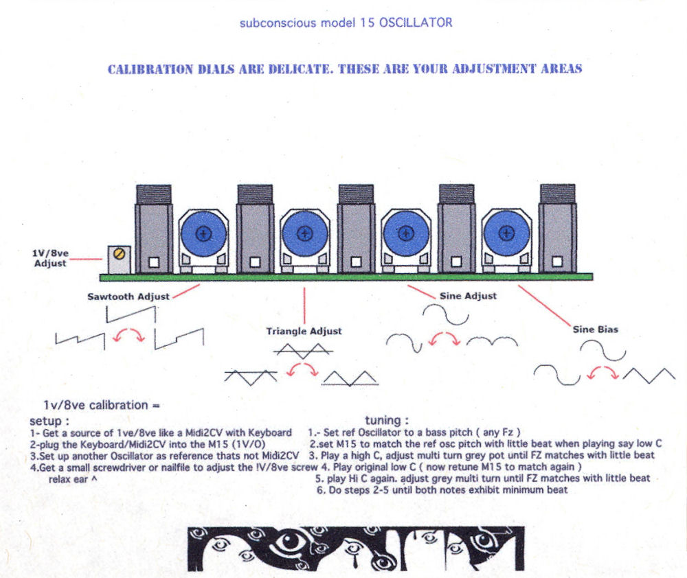
is apparently a Rev 2.0 module which did not have the trimpot. [For completeness, here is a scan of the Subcon M15 calibration 'card' that was apparently sent out with each module.] Having seen photos of a Rev 2.0, it appears all four boards in the assembly underwent changes to become 'rev 2.1': clearly the sine ampl pot was added, and the three parallel boards also have much higher 'arches' away from the main PCB at the 2.1 versions, presumably to increase clearances from components on the main PCB (and I'm assuming here that the three smaller boards would have changed 2.0→2.1 at the same time as the main board did—compared to my rev 2.4, there are other tracking differences in the main PCB from the 2.0, but these could be other changes made at 2.2-2.4!). Note 2. Post #720 Model 15 Sine Wave modification procedure, Oct 25, 2006:
I've outlined the procedure for updating Model 15 boards rev. 1.2 thru 1.4 with the sine wave improvements which were introduced with the rev 1.5 release. You can see them here: http://www.ear-group.net/sinemod.html Please note: This won't work with M15's that are 1.1 or below. There may be another procedure for that, but this is a bit more complicated. Also note that you do not need to do this on rev. 1.5 and above - it's already in there.Unfortunately, as of mid-2013 the ear-group.net website seems to no longer exist, the link above with it: the Wayback Machine has captured that page, but again unfortunately the many photographs it references aren't there: http://web.archive.org/web/20120801094731/http://www.ear-group.net/sinemod.html. Sinewave circuit evolution: the original/Rev 1.1 circuit is essentially the same as the Rev 1.2-1.4, albeit with some component value differences; the change at Rev 1.5 brings it almost in line with the later Rev 2.x version (it wasn't complete until the addition of the 'Sine Ampl' trimpot mentioned above); on examining a Rev 1.2 close up, the instructions referenced above for retrofitting the changes to Rev 1.2-1.4 boards do make sense (without the photos); whilst the component locations concerned didn't change much between Rev 1.1 and Rev 1.2, there are several 0Ω links replaced with PCB traces in going from single-sided to a double-sided PCB (making things harder to tally-up), but the main thing stopping the mod being retrofitable to the Rev 1.1 is the absence of the ability to trim out the DC from the triangle wave, an enhancement that appeared in Rev 1.2 (it would not be beyond the realms of plausibility to add the necessary trimpot, but it would require some precision track-cutting to achieve it). Note 3. Post #2437 New Model 15s: new jacks for the 'wireless' design, Jan 23, 2009:
Effective today we are beginning shipments of the newly re-designed Model 15 Complex VCO which incorporates two major changes: The elimination of Cliff Jacks and 12 point to point interconnect wires. A photo has been posted: << This is the photo above. >> The circuit, the module functionality and the price remains unchanged. These improvements were put in play to increase our production throughput, decrease the potential for field failures with the elimination of the 12 hand-soldered wires and addresses the continual Cliff jack availability issue which has shut our production line down in the past, most notably last summer at the worst possible time imaginable: two weeks before the ELFs were to be released when Cliff announced they were halting worldwide production for three months. Freed from those constraints I am confident the M15 availability will flourish. Note 4. Photo showing expo conv now on main board (bottom left corner), and smaller analogue switch IC (second IC up), from thread How can I fix a blown Plan B Model 15 rev 1.2 ? at ModWiggler. See also Note 10. Note 5. Photo (in same thread), showing that the tempco is a through-hole device, tucked-up underneath the matched pair (6-legged can bottom right). Note 6. Photo (again, same thread), comparing Rev 2.5 PCBs, both with and without the power-reversal protection. Note that this also means that there are two different PCBs with a 'Rev 2.4' designation: one for the Rev 2.x configuration, the other for the Rev 2.5... Note 7. In comparing the circuits, I noted 22 component differences (and this doesn't include that all pots are changed): the majority of these (16) occur in the acknowledged changes to the PWM & morph circuits, and the sine shaper (the Vactrol type in the morph circuit is changed from VTL5C2 to VTL5C3 too). Of the half-a-dozen (apparently unacknowledged) changes in the CV processing/oscillator core, two at least have the potential to impact the basic operation of the VCO (e.g. the tracking): there are reports of people finding it difficult to calibrate their units, but accurately quantifying the impact of the changes is unlikely to be straightforward. It is possible that there are two different PCBs with the 'Rev 4.0' designation on them. My unit (#74/110, and marked Rev 4.0) has clear vestiges of an attempt to incorporate a 'high frequency trim' circuit: thru-hole footprints for a resistor and trimpot, and silkscreen designations for two other resistors, but with their footprints deleted and some tracks left dangling in 'mid air'. This post includes some detail of a 'progress update' from Subcon, including this screenshot of the PCB layout, clearly showing these same 'Optional HFC' components, and a comment alluding to it: "I've been told of other secrets on the board for super users, but that is a secret. isn;t it?" [sic]. This photo (which was linked from this post, but has gone now), shows that the holes are present in unit #10; here is a composite photo showing the layout, top and bottom of my unit, and unit #10, showing 'initial intent', 'not present', and 'present'. Finally this photo from this post shows that the holes are again not present in unit #5—so clearly two different PCBs exist, but no clear indication of which came first (two early units exhibiting both PCBs), and an apparent later unit, #74, with an early designation, '4.0'. Note 8. As well as the vactrols being moved, other little 'tidy-ups' have been made: in the rev 2.4/2.5 there were 10 discrete wires running between the two PCBs, mostly being the wiring for the pots; in the 2.5/2.5 these have all gone, and the number of headers between the boards has increased by one to five, so presumably between them these now carry the signals that the wires did, as well as those for the vactrols, having moved to the other board (this makes working on the 2.5/2.5 much easier, as aligning the wires on a 2.4/2.5 during re-assembly was something of a challenge!) Note 9. On the Rev 1.3 the tempco changed from a through-hole to a surface mount device, but curiously it is on the solder-side of the board, along with the LS318 matched pair, which fits snuggly over the tempco. The import of this was initally lost on me until I had occasion to compare the 1.3 layout with a photo I had taken of the 1.2 board, and immediately realised that on the 1.3, the two layers on the board are reversed, i.e. what is the bottom layer on the 1.2 is the top layer on the 1.3 (and vice versa for the other layer). It is possible this was merely a batch problem (in my job I have seen four-layer boards where the PCB fab house have unintentionally switched the inner two layers—the boards worked fine of course, but looked quite odd in a side-by-side comparison with a 'good' board!). This is illustrated in this photo, which is a mirrored image of the bottom of a rev 1.2, and so it looks as it would if you could see through the PCB to it from the component side, next to a silhouetted image of the top of the rev 1.3, from which it is evident that the trace pattern is very similar (the latter looks a little weird, as I've done a 'perspective straighten' on it to account for the angle it was taken at). Could it thus be that the rev 1.3 to 1.4 change (wholly or partly) consisted of rectifying this switch in layers (so the LS318 plus tempco would have been back on the solder side, and thus wouldn't have presented anything of an exception as they appeared to on the rev 1.3)? Note 10. The larger MAX333 analogue switch chip used in the original batch of Rev 1 M15s was apparently replaced specifically by the Maxim DG212 in the Rev 1.2 design. The Maxim version of this chip does not require a 'VL logic supply' voltage at pin 12, so the rev 1.2 design leaves the pin unconnected (it is IC6). This meant the use of other makes of chip, such as Analog Devices and Vishay Siliconix, was unnecessarily excluded, as without a suitable voltage at pin 12, the tri-to-saw conversion (the chip's function) will not work, and a tri wave will be output instead of a saw. I don't know at what point this was recognised, but my Rev 1.3 has what looks suspiciously like a factory-fitted mod, in the form of two resistors soldered under IC6, to rectify this situation. By the time of Rev 1.5, these two resistors were properly incorporated into the PCB design—it is very possible that this actually happened at Rev 1.4. [Page last updated: 08 Aug 2022 |
||||||||||||||||||||||||||||||||||||||||||||


