Personal web pages ofTim Stinchcombe |
A-110 Sine Wave ModificationThis modification came about following an enquiry at the Yahoo! group as to whether it would be possible to improve the sine waveshape from the A-110 VCO. Some research into tri-to-sine waveshapers uncovered the circuit used here, and as it was so simple and would be easy to implement, I decided it was worthwhile pursuing further. Dieter Doepfer has suggested that he might be prepared to make a small PCB to allow others to more easily modify their A-110s: if this actually comes about, I shall amend this accordingly, but I should point out from the start that there quite a few issues addressed below which may mean this is far from being a certainty! (Not least of which is how those without access to an oscilloscope might make the adjustment to get the best sine waveshape.) The modificationThe basis of the mod is straightforward: remove the components currently doing the waveshaping; build a small board with the new circuit on it; wire the new board into the A-110. Here is the circuit showing the component values I finally decided on (the pot is a preset): 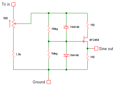
The components to be removed are all located at the bottom edge of the A-110 PCB, and are: D1, D2, C9 (1n), R52 (47kΩ), R42 (220kΩ) (the A-110 schematic can be found in the A-110 Service Manual at Doepfer's website). In addition R43 should be changed to 24kΩ (from 47kΩ) to reduce the gain of O4, the final sine output stage, and a new 470pF capacitor is also added (see below). The new components were mounted on a little piece of stripboard: only a single track cut is required, at 'X' in the photo:
The last thing I did was add a 470pF capacitor to the sawtooth-to-triangle conversion circuit:
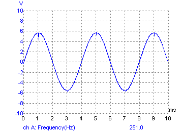
Setting up: my Picoscope is capable of displaying a spectrum, and can give a THD calculation too, thus simply adjusting the pot until I got the lowest THD reading was all I needed to do; using just a scope trace makes it a little harder, as it requires 'visual judgement' as to where the best sine shape is obtained; without a scope, one would have to do it aurally, i.e. use one's ears to decide the point where the minimum of harmonics can be heard. Output tracesThe following three traces show the sine output at frequencies of approx, 8Hz, 250Hz and 4kHz: 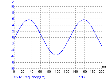
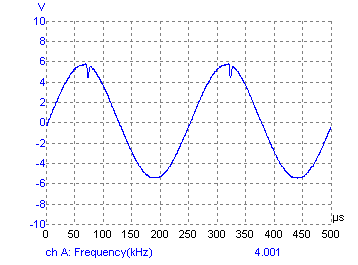
This is the spectrum of the 250Hz trace, showing a THD of below 1%: 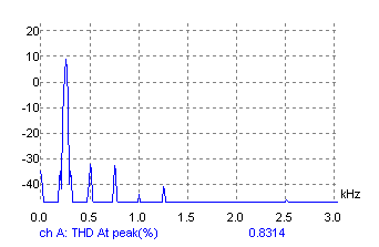
Perhaps a more useful comparison is the following: I imported the 250Hz trace data into SIMetrix and compared it to a sinewave from a transient run of the same parameters—it is a good visual comparison of how accurate the sine waveshape from the A-110 now is!: 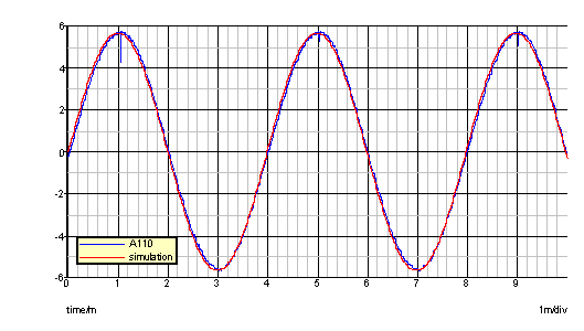
Here is a comparison of the 'glitch' in the triangle wave, as modified by the extra 470pF capacitor (blue trace), against my other (unmodified) A-110 (red trace) (oscillators running at about 1kHz): 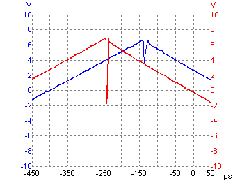
Finally, here is a comparison of the sine output between the modified oscillator and the unmodified one: 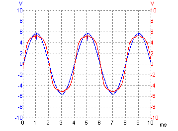
Design issuesAmplitude/waveshape adjustment: for the circuit to work well, the peak amplitude of the triangle input must be set very precisely, to a factor of about 1.8 times the pinch-off voltage of the JFET used. Most of the circuits I found used a ±10V triangle input, had a 10kΩ pot for adjustment, and used a 2N3819 JFET which has a pinch-off voltage possibly as large as −8V. The A-110 triangle is roughly ±6V, so the JFET pinch-off voltage needs to be in the region of 6/1.8=3.3V, so I chose to use a BF245B whose pinch-off range is from −1.6V to −3.8V. Using a 10kΩ pot also didn't work very well: because of the loading effect of the circuit, the adjustment isn't very linear, having a steep slope around the point where the adjustment is needed (around about 4V). The following simulation trace shows the effect:
Also shown is the curve for the arrangement used, a 1.5kΩ resistor with a 500Ω pot, showing the much gentler slope, and hence finer adjustments are possible. (But lowering the total resistance in this way leaves us vulnerable to the next problem...) The range of adjustment possible should also mean that it will cope with the wide range of pinch-off voltages possible for candidate BF245B's! Clipping of triangle output: the total of the two 150Ω resistors and the FET 'on' resistance, in parallel with the adjustment pot, presents quite a large load to the triangle wave output op amp (O3)—so large in fact that it is possible to severely limit the available output swing of the op amp to the point where it actually clips the triangle, and consequently the sine wave also. The point at where this happens will depend on both the values chosen for the adjustment pot and the load attached to the triangle output: for the values shown this became a problem when the load on the tri output was about 4.5kΩ, which equates to about 4 'standard' A-100 inputs being driven (i.e. inputs taking the signal through a 50kΩ pot). Symmetry: the circuit is also affected by any asymmetry of the input triangle wave, and several of the circuits I found include a trimpot to compensate for this (a 10k or 100k pot across the supply rails, wiper through a 5.6k resistor also going to the 'tri in' node). However in the A-110, after the main saw-to-tri conversion there is a coupling capacitor which takes the DC out—there is still a small amount of asymmetry in the triangle wave, but on the module I modified this didn't seem to be enough to warrant putting the extra trimpot in (but I did leave space for it on the stripboard): it is hard to see any asymmetry in the sine wave which would need removing. Notes on the circuitI first came across the circuit in Electronotes, but then found it was mentioned in quite a few books (see refs below): few attempt to explain precisely how it works, or detail what the resistor values might be related too. Thankfully the actual paper provides some of the answers: the 1MΩ gate resistors are not critical, as long as they are high enough not to load the signal, and low enough to forward bias the diodes; the diodes themselves are not critical either, preferrably being of the same semiconductor material as the FET (the possibility of this not being the case presumably more likely in 1965 than it is today!); the drain and source resistors should be equal, and the same as the FET drain-to-source resistance at zero gate-to-source voltage (from the Philips BF245 data sheet, for a BF245B this is somewhere between 100Ω and 200Ω, so 150Ω seems a reasonable value). In order to work effectively the amplitude of the input triangle wave needs to be just right: in the initial analysis in the paper they give the relation Vm/Vp=1.33 (repeated in one of the Electronotes articles, and other references citing the paper), where Vm is the peak amplitude of the triangle and Vp is the pinch-off voltage of the JFET. Simple simulation shows that this relation is clearly erroneous: VTO of the Philips BF245B SPICE model I am using is −2.31; multiple transient runs give Vm for minimum THD at around 4.04V, giving Vm/Vp=1.75. Indeed even their own experimental data (the figure at the top of p101) suggests a ratio of about 1.66. As is usual for a journal paper, the workings are very terse, and so far I have been unable to replicate all of their algebra—the situation is also complicated by the fact that they give most working for an idealised version of the circuit (a bridge-rectifier feeding the JFET, the gate conected directly to source); they then introduce the source and drain resistors (the bit I'm struggling with); and then for the practical circuit they ditch the bridge, and introduce the diodes/resistors on the gate (for which no additional working is given at all). It would be interesting to see if any later papers have commented on this apparent anomaly ( ReferencesRD Middlebrook & I Richer, 'Nonreactive filter converts triangle waves to sines', Electronics, vol 38, March 8 1965, pp96-101. Electronotes: the circuit appears in many places: #7(page 6), #28(6), #36(5), #39(6), #75(7), #123(3) (THD measurement), AN115, and The Musical Engineers Handbook, section 5b(18). H Chamberlin, Musical Applications of Microprocessors, Hayden, 1985, pp192-195. B Klein, Electronic Music Circuits, (published by the author), 1995, p94. RF Graf, Converter and Filter Circuits, Newnes, 1997, p118: this is referenced as being sourced from: Linear Data Manual Vol. 1: Communications, Signetics, 1987, p4-311. [Page last updated: 29 Aug 2010] |