![]()
|
|
Personal web pages ofTim Stinchcombe |
Be wary of what SPICE simulation tells you!Introduction and background: I have always found SPICE simulation incredibly useful, and as it does have a certain reputation for occasionally producing misleading results which can trip-up the unwary, I usually try to put a little extra effort into understanding what it is doing, in the hope that I might spot something which isn't quite 'truthful'. In this instance though I feel I have had my fingers well and truly burnt, and I thus offer it up as an example of what can happen if you are not paying attention closely enough! Some years back I decided I would emulate the lower resonant peak of the TB303 diode-ladder filter in the ladder filter I was then designing. This required placing a second-order high-pass filter in the feedback loop, which used an LM13700 operational transconductance amplifier (OTA) [ref 1] for voltage-control of resonance, and one pole of this was easily accomplished by simple first-order RC-sections on the inputs to the OTA. I thought I could use the DC level-shifting capacitor feeding the signal back into the ladder for the second pole, but it didn't look very promising in simulation runs. No problem I thought, and without thinking I simply stuffed another capacitor at the output of the OTA, in front of the resistor there, completely oblivious to the fact that was not-a-very-good-idea. I ran a load of simulations, and these showed there was a high-pass effect at around the point I had expected, and so I thought I was up-and-running! The breadboarded filter made some interesting sounds, especially when the gains of the OTA were cranked up and the circuit was clearly resonating at both the deliberately-designed-in lower resonant peak and the usual one at the (higher) low-pass cut-off frequency. However something was not right with the cut-off frequencies and the gains, which at the time I couldn't fathom out—the reality and the calculations just didn't seem to match up—and so the project was put down, and other work took over. Some seven years later and I decided to have a more determined look back over the design, and on doing so I immediately spotted the naivety of what I had done in my previous un-thinking state: since the OTA outputs current, and this same current will flow through both the capacitor and the resistor at the output of the OTA, there should not be any high-pass action there at all—at least assuming the OTA output voltage doesn't doesn't max-out at either rail, in which case all bets are off! (Thus it is quite likely we will get clipping as the capacitor forces the output voltage of the OTA to limit just inside either power rail.) So the question arises: how was SPICE so effectively able to collude with my naivety and fool me into thinking I had the high-pass effect I desired? The answer to this question was obviously going to require a detailed knowledge of the internals of the SPICE macromodel I was using for the OTA, and as it turned out, a good deal of effort too! In my simulations I generally use the original National Semiconductor SPICE model for the LM13700, which I have uploaded here for convenience (the original is available here at the LM13700 product page at TI, who bought-out National some time ago). There is also a useful component-level model here, from one of the original designers of the LM13600/13700, and so I expect that it would also be a reasonably accurate model. I've had a working familiarity of the macromodel for many years, and whilst it is possible in SIMetrix (my SPICE simulator of choice) to probe voltages and currents inside subcircuits, it was going to be a lot easier to work from a schematic of the model, so I converted the netlist to a schematic (SIMetrix has a built-in script which makes this a little easier to do): click the image for a better resolution version—my method of generating an image from the schematic is a little 'clunky':
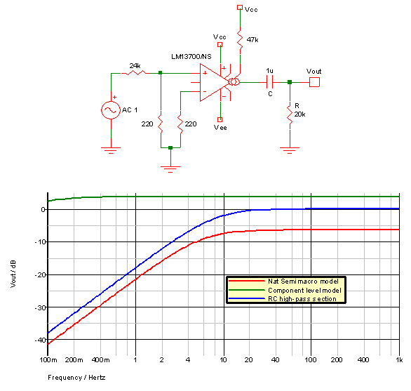
The Problem. The circuit investigated here, for convenience, is a slight simplification of that in my original filter: basically the circuit is stripped back to the simplest form that exhibits the problem, as shown in the following image:
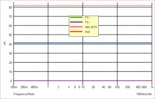
The red trace exhibits the problem—it looks like we do have a high-pass filter. The green trace is from the same set-up, only using the component-level SPICE model instead: notice the lack of a corner in the middle of the trace and a different final gain level (it will be noticed that there is some roll-off at the very left of the trace—I haven't traced the exact cause of this in that particular model, but that it is two orders of magnitude away from the area of interest, had I been using that model at the time there would have been some hope I would have been alerted to the mistake sooner!). The blue trace is from a simple high-pass RC combination of a 1μF capacitor in series with a 20kΩ resistor, to show where I was intending the cut-off to be: it calculates at 8.0Hz; the red trace is at 5.6Hz, which to all intents and purposes, is pretty much the same value. Thus perhaps I can be forgiven for thinking that I had what I wanted, and thus why I was fooled! Basic operation of the macromodel. For those not familiar with the workings of SPICE macromodels the one being studied here may look a little unusual, as they frequently bear little resemblance to the circuits they emulate. They can look more like a small-signal analysis equivalent circuit, as they often make use of idealised circuit elements such as current sources, transconductance gain blocks, and so on. Understanding how SPICE macromodels work is a skill that takes a little practice, though the Nat Semi LM13700 model is perhaps easier to grasp than many standard op amp macromodels, as there are few frequency-dependent circuit elements. (Ref [5] is an excellent book on SPICE macromodeling; refs [2, 3 & 4] are other useful books on how SPICE works in general.) We start with the amplifier bias current pin, Iabc, at which the model has two diodes in series with a voltage source, D5, D6 and V3. The artifice of the zero-volts voltage source V3 is that it measures the current through itself, and passes this as the control current into current-controlled current source (CCCS) F3—thus the amplifier bias current is directly mirrored into the tail of the differential input pair Q1 and Q2, equivalent to the actual circuit, though it is a behavioural equivalence, hence the two diodes plus current source behave the same way as the transistors of the current-mirror of the real circuit, rather than copying the exact circuit topology itself. The input stage consists primarily of transistors Q1 and Q2 and the linearizing diodes D1 and D2, which all behave in the model as the real IC, so require little further explanation (and the diodes are not used in the circuit in this investigation—no diode bias current is applied—and so they aren't considered any further). Zero-volts source V6 measures the input bias current into Q1, which is used to generate an input offset current via source F1—this contributes to a small 'imbalance' seen at the input, but the majority of the imbalance comes from the difference in the IS parameter, the saturation current, used in the transistor models QX1 and QX2 used for Q1 and Q2 respectively (IS=5E-16 & 5.125E-16 resp.). There are a further two current-measuring zero-volts voltage sources, V1 and V2, in the collectors of Q1 and Q2, feeding a further two CCCSs, F4 and F2 respectively, which form part of the output stage—both the current sources have slightly larger than unity gain (×1.022). If, for the moment, we ignore F5 and the diode/voltage structures at D7 and D8, we see the simple operation of the model in emulating the real chip: the current at F4 subtracts from that at F2, so when the positive input voltage is greater than the negative input, F2 is greater than F4, and the difference is sourced out of the output pin (and when the opposite is true at the input, giving F4 greater than F2, the chip sinks the current difference, i.e. current is into the output pin). The other CCCS F5, (voltage-controlled) current source G1, and V7, represent the output resistance, by sinking a current proportional to both the voltage at the output and the amplifier bias current (it looks to me that G1 and V7 are really just a little 'programming trick' to get the output voltage into a format suitable for passing into the polynomial in F5). The two diodes D7 and D8 and their associated voltage sources, V4 and V5, serve to limit the output voltage to just inside the supply rails—for example, when the output voltage rises to about a diode-drop above 1.4V below the positive rail, D7 will start to conduct and effectively clamp the output voltage at that level (D8 works similarly in conjunction with V5). Identifying the culprit. The circuit to be investigated is the simple one shown above, but for convenience we use the expanded schematic-version of the LM13700, also shown above (this makes probing around the LM13700 much more accessible)—the combined circuit used is shown here. By the very nature of a transconductance amplifier it is the currents that are the principal actors, so that is where we start. The defining equation for the OTA output current, given the voltage difference ediff across the input terminals is: Iout = 19.2×ediff×Iabc, where Iabc is the amplifier bias current. (This ignores the predistortion diodes, which we are not using, and is basically equation (5) in ref [1]—something very similar often appears in other OTA datasheets.) For our set-up we have a 47kΩ resistor, which is virtually across the supply rails, providing Iabc: more precisely, assuming both the diodes at the Iabc pin drop about 0.7V, then we will get Iabc = (24-2×0.7)/47k = 481μA. For the moment we will short out the 1μF capacitor on the output (C8), to remove any frequency dependence on the output current, and check the current, and then work back towards the input. The standard AC source applies a 1V magnitude signal, which is attenuated by the 24kΩ:220Ω potential divider on the input = 1/110, so we expect to see Iout = 19.2×1/110×481μ = 84μA being output. This is the red trace in the following (it is about 82μA, close enough):
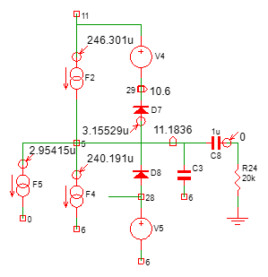
However, if we look at the currents in the sources F2 and F4, the green and blue traces, we notice what seems to be an 'anomaly'—they are very nearly equal at about 42μA (I have tweaked the plot a little to separate the two lines!). The sign sense for the probing is the same, so it looks as though the output current ought to be zero. This is our first lesson: we are performing an AC analysis, so currents and voltages are complex entities, i.e. they have both magnitude and phase, and the simple current probing is clearly just giving us the magnitude in the absence of us asking for anything more. If we specifically probe the current phases we do indeed confirm that they are 180° out from each other, and hence add rather than subtract, and so the 84μA is confirmed! Next if we expect to see the 481μA of Iabc mirrored into source F3, we are in for another surprise—the mauve line is 0, zippo! Again this is because of the way SPICE works: an AC analysis works by first finding all the DC bias points in the circuit, it then linearizes non-linear circuit elements (e.g. diodes, transistors etc.) about these bias points, and then does its calculations. Because there is no AC component to Iabc (the AC source used is only connected to the one OTA input terminal), the plot of Iabc reads zero. Turning to the differential pair at the input, these same issues apply: the AC collector currents will be nearly the same as those in F2 and F4 (ignoring the '×1.022' factor), i.e. they are 40-odd μA, and of opposite phase. We should now, however, start thinking about the DC components of the signals. We are applying a (DC) current of 481μA for Iabc, and this will be mirrored in source F3 in the tail of the differential pair. As there is essentially zero DC input at either base of the input pair (ignoring effects due to input bias currents etc.), this current splits roughly equally between the collector currents of the transistors, and as can be seen in a moment, the currents in F2 and F4 are also nearly equal, at roughly 240μA each. The calculation of the AC components of the collector currents is a deviation, plus in one collector, minus in the other (hence the 180° phase difference) due to the AC voltage amount applied at the bases (the AC source, magnitude 1V, attenuated by the input potential divider, 24k:220Ω): the expression for this is basically half that given for Iout above, which in fact derives directly from the calculations surrounding the differential pair (see, for example, my account in Section 2.1.1, leading to equations (6)-(7), in [6]). I think there is little doubt that it can be quite confusing trying to get one's head around all of this! So let's run a standard SPICE DC Operating Point analysis on the circuit to check the relevant DC bias points. This image shows a part of the circuit with some currents and voltages annotated ('arrowed circles' are the currents into that pin; the little 'box arrows' are the voltages at that node). Note also that I have now put capacitor C8 back in so that we can observe its effects:
First we note that the currents in F2 and F4 are roughly equal at some 240μA each (as mentioned above); the small approx. 3μA in F5 is for the output resistance (it is an easy matter to remove this altogether to show it is not having any significant effect on the deleterious high-pass effect we seek); also note that there is no current in the deviant capacitor C8, which is because SPICE treats capacitors as open circuits when doing its DC operating point calculations. Next we may observe that the voltage at the output is rather high, at 11.18V: the DC operating point calculations have decided that the output will saturate near the positive supply rail. Worse than that, diode D7 is conducting: it is dropping 584mV, and has just over 3μA flowing through it! This means that from the perspective of a small-signal, linearized equivalence for use in AC analyses, it behaves like a resistance—this then is the culprit! Evaluate the culprit. We can replace any diode at its operating point conditions with an idealised set-up consisting of a voltage source, an ideal diode and a resistance:
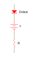
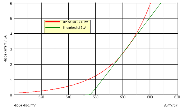
Generally a diode's I-V curve is a smooth exponential increase; one of its SPICE parameters is N, the emission coefficient which appears in the denominator of the index of the exponential function, and its default value is just 1; by making it small, say 0.01, the index of the exponential becomes very big, giving an extreme exponential curve which very rapidly changes from 'small' to 'very big'. Thus when the voltage across the whole exceeds the voltage source, the ideal diode suddenly conducts, and the I-V curve is then linear, due to the resistor (if it weren't for the resistor, it would shoot up vertically). Thus I used the (very simple) diode model of the LM13700 macromodel, '.MODEL DX D (IS=5E-16)' (most of the diode SPICE parameters thus assume their default settings), and plotted an I-V curve, the red trace:
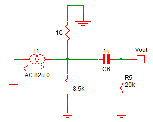
I then estimated the tangent to the curve at the 3μA-584mV point, and came up with a value of 8.5kΩ for the resistor; I stepped the voltage source so that I-V curve of the idealised set-up, the green trace, more-or-less just touched the red one at that point (the exact value of the voltage source isn't particularly crucial as we don't need it for the following AC calculations!). (The ideal diode model is just: .MODEL Dideal D (IS=5E-16 N=0.01) ) We can now make up an equivalent circuit for the output stage, including the deleterious capacitor and resistor at the output, which shows exactly how the high-pass effect originates, and thus why I got fooled in the first place: we replace all current sources with a single (AC) source outputing the 82μA we know we have; diode D7 is replaced by just the 8.5kΩ resistor. (I've shown D8 as a 1GΩ resistor—it's not really needed at this level, but at a few steps 'further back' which I've not expounded here, I needed a 'DC path' replacing the diode in order to get the DC operating point calculating correctly, so it stays in as a little aide memoire for this fact! Note also that I've swapped the relative positions of D7 and D8 from 'above'↔'below', and that they now run to ground, as this is for use with AC analysis, and hence the DC voltage sources V4 and V5 don't matter):
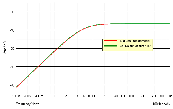
It is not too difficult to see that this is indeed a high-pass filter, nor in fact to do a little algebra to confirm this fact, and if we compare the response with that of the one showing the problem, we can see that it is pretty much bang-on:
The pole causing the cut-off turns out to be from the 1μF capacitor coupled with the 8.5kΩ (for D7) plus the 20kΩ output resistor, which gives 5.6Hz. Annoyingly this depends strongly on the 3μA flowing in D7, which derives from the differences in parameter IS for the input transistor models—had these two values, 5E-16 & 5.125E-16, been chosen to have been slightly different from what they are, then this may have moved the pole sufficiently that I would have been alerted to the fact that I had done something stupid sooner. I've not really checked what the waveforms in the real filter actually look like, but I expect there is an inordinate amount of clipping/voltage compliance effects etc. going on. SPICE can be incredibly useful, but this is a prime example of how it always pays to be aware of its limitations, to find out why things go wrong when they do, and to learn from them in order to be better prepared for the next time! I guess this instance is a classic case of 'Garbage in, garbage out'! References: 1. LM13700 datasheet at Texas Instruments. (Equation 5 is basically the expression that I use above—however I find the algebraic development there a little fraught, as there are several places where particular attention is needed as to whether signals are single-ended or differential, as this leads to a perceived 'factor of 2' error.)2. Inside SPICE, Ron Kielkowski, McGraw-Hill, 2ed. 1998, ISBN 0079137121. A very accessible book on how SPICE actually works, explaining the different anaysis modes etc.3. SPICE Practical Device Modeling, Ron Kielkowski, McGraw-Hill, 1995, ISBN 0079115241. Perhaps a little more specialised than the one above, but it gives good insights as to how the device models work.4. The SPICE Book, Andrei Vladimirescu, Wiley, 1994, ISBN 0471609269. This is my go-to reference book when I have a query about SPICE syntax, or need to know what the actual device caclulations are.5. Macromodeling with SPICE, J. Alvin Connelly & Pyung Choi, Prentice Hall, 1992, ISBN 0135449413.6. Analysis of the Moog Transistor Ladder and Derivative Filters, TE Stinchcombe, 25 Oct 2008.[Page last updated: 24 Feb 2024] |