![]()
|
|
Personal web pages ofTim Stinchcombe |
A-150 Large Signal ModificationOlder versions of the A-150 module used the '4053 analogue switch chip, which is restricted in the size of the voltages it can handle. If a signal greater than about 8V (or less than -8V) is applied to one of the switch channels, circuitry in the module intended to protect the chip from large voltages allows the signal to 'bleed-through' to the output, thus making that channel appear to be on, when it should actually be off. This originally arose at the Yahoo! group several years ago, where the context was of switching gate/trigger type signals (up to approx the 12V rail), as opposed to audio signals (which generally within Doepfer modules are within ±5V amplitude): the modification here allows signals of greater than 8V to be switched by the module without the bleed-through problem, but in so doing such signals become limited to 8V (and bipolar signals - swinging between -8V and about +7V - can still be switched). Note that the newer version of the module, which uses the DG409 analogue switch chip, correctly handles voltages right up to ±12V. Note also that Doepfer have a mod for this problem on the 'FAQ' page at their website (but note that their solution shifts the whole supply to the chip from ±8V to 0-12V, and so the module is then no longer capable of switching bipolar signals: however unipolar signals are then not limited as the solution presented here!). The cause of the problem is the way the protection diodes (D1, D4 & D5) are connected from the In/Outs and the Out/In up to the +8V rail (there is a schematic of the A-150 on the FAQ page of the Doepfer website): these protect the chip by preventing not much more than 16V being applied across it. However the diodes only conduct when the signal applied is a diode drop above the +8V supply, so the voltage at the chip in/out is then more than the chip supply: this causes internal pn junctions in the chip, which under normal use are reverse-biased, to become forward-biased and thus to conduct, causing unwanted signal paths in the chip. The basic idea of the mod is thus to simply lower the voltage that diodes D1, D4 & D5 are connected to, by placing a resistor and 6.8V zener diode across the 8V supply, and tying them to this new voltage. This will thus stop voltages greater than the supply voltage of 8V reaching the chip when large signals (such as gate/triggers) are applied to the switch. I only carried out the modification to the top switch in the module (the left circuit on the board): extending to modify both switches just means cutting 3 more tracks and adding 3 more wires (i.e. it does not double the work needed!). The new components needed are:
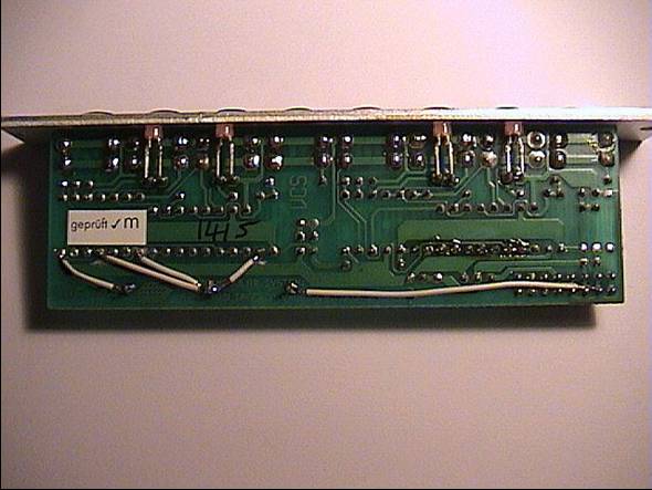
The following photos show my modified module:
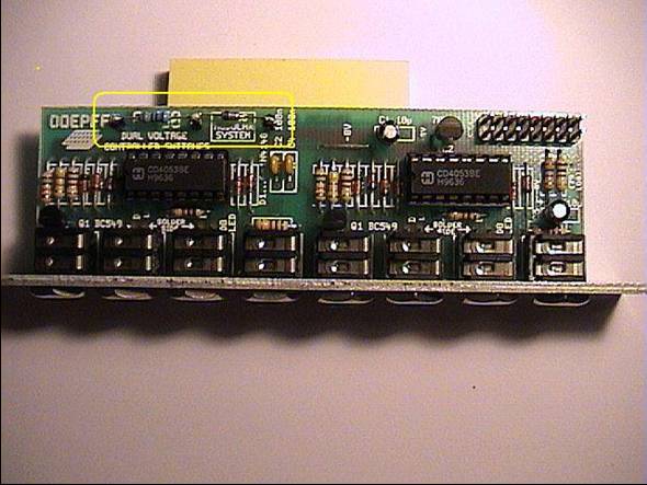
Identify the following on the board (hold so that 'DOEPFER A-150' text on the component side is the right way up):
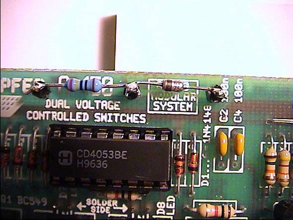
Drill 3 holes in a straight line, suitable for insertion of the pins, about 3 to 4mm in from the top edge and about 15mm apart (but not too close to the +8V rail on underside). Call the pins 'left', 'middle' and 'right': I placed the left one through the 'R' of 'DOEPFER'; middle one between the '0' of '150' and the rectangle around 'A-100 modular...'; and the right one between the rectangle and 'C2 100n'. Before inserting the pins, cut the tracks (scrape away the copper using a sharp pointed object, like a penknife: hold the board up to the light to check that the track is actually cut):
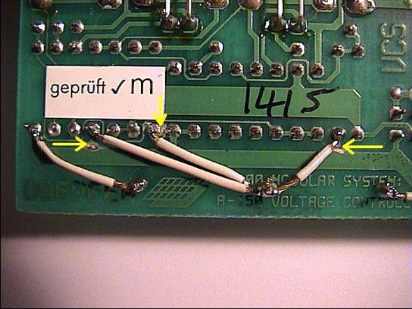
Insert the pins (using the JW59P pins, I put the little plastic lug on the component side, so that the longer end projects on the solder side of the board). Solder wires on the underside of the board, from the projecting end of the appropriate component to the appropriate pin:
On top of the board, solder the 240Ω resistor between the left pin and the middle pin. Solder the zener diode between the middle pin and the right pin, with the black stripe nearest the middle pin (again, probably best to solder the resistor and zener to the middle pin in one go, and again take care not to overheat the zener!). That's it for modifying the left switch. To do the right switch as well, cut the tracks where the diodes D1, D4 & D5 of the right circuit connect to the 8V rail, and attach wires from the diodes to the middle pin. To summarize, you should have the following: +8V supply from R2 to 240Ω resistor at left pin; 6.8V at middle pin (junction of resistor and black stripe end of zener) to black stripe ends of diodes D1, D4 & D5, which are disconnected from the +8V rail; non-stripe end of zener at right pin to ground at power connector. Check: all cuts really are cut; no tracks unintentionally cut; no stray blobs of solder bridging any tracks. To test I suggest something like the following (if modifying one switch, you can check against the unmodified one; if doing both, a 'before' and 'after' test would probably be a good idea!). Patch a suitable CV source to the switch CV (e.g. A-129/3, A-174, A-176); an LFO square output to A-160 'trig in'; 160 'divide by 2' output (so this is now 0-12V) to I/O2 on A-150; O/I to CV2 on A-110, listen to an output of the VCO. With I/O1 unconnected, regardless of the switch position, on an unmodified switch you should be able to hear the alternating pitch due to the 0-12V pulses (cut down to about 8.5V) always coming through the switch (adjust LFO frequency to a suitable slow rate). If you ground I/O1 i.e. attach a CV source at 0V, the affect is much less when the switch is 'open', but you can still hear some variation in pitch caused by the bleed-through. After the mod, you should only hear the pitch change when the switch is 'closed', i.e. when the clock signal is switched through; in the 'open' position the pitch should now be steady. The voltage swing of all signals passing through a modified switch will be limited to about 0-7.5V. For gate/trigger type signals I don't think this will unduly load the circuit which sources them, and judging from most of the Doepfer circuits I've looked at, it is unlikely to prevent the gate/trigger signal from doing what it should at its intended destination. (The mod doesn't alter the negative supply, therefore the bleed-through problem is likely to remain should you try and switch signals less than -8V.) Note also that this modification increases the power consumption of the module by about 5mA. [Page last updated: 14 Dec 2009] |