![]()
|
|
Personal web pages ofTim Stinchcombe |
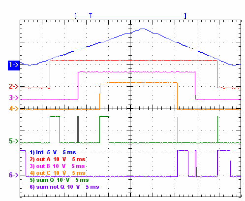
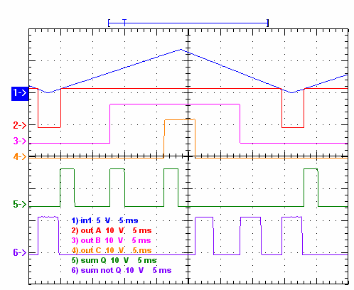
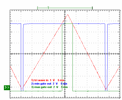
Plan B M17 Triple Event Timer modificationsAbout the first thing I noticed after I plugged my M17 in for the first time was nasty little extraneous pulses coming out of the 'A+B+C' output. Of course, on further investigation, I discovered others had already raised this problem some years ago in the online forums; another little 'annoyance' mentioned about the module was that by allowing the threshold levels to be set all the way up to over 10V, much of the pot travel is wasted when used with smaller input signals, i.e. from those that max-out at around 5V, being typical of many LFOs and EGs out there. Once their causes were understood, both problems were relatively easy to overcome, and details of two simple mods are given here. Note that all that follows applies to the Rev 2.0 PCB, which is what mine is—I have no idea how different any preceding revision levels of PCB are! [And in a slightly nit-picking vein I note that the 'A+B+C' output is somewhat misleadingly annotated: the 'A+B+C' output is clearly not literally the logical 'or' of the three individual outs, but we do get a pulse out at the rising edge of either A or B or C; similarly we get a pulse out of the 'A+B+C' output on the falling edge of either A or B or C, i.e. it is not so much 'not the sum' of the outs, but it is the sum of the 'not outs', and thus perhaps would be better labelled as 'A+B+C'?!] 'Sum out' modificationThe problem manifests itself as narrow pulses output on the 'A+B+C' output, aligned with the falling edges of the main gate outputs, 'A', 'B', and 'C'. These are seen in the right-hand end of the green trace 5 in the following set of traces:
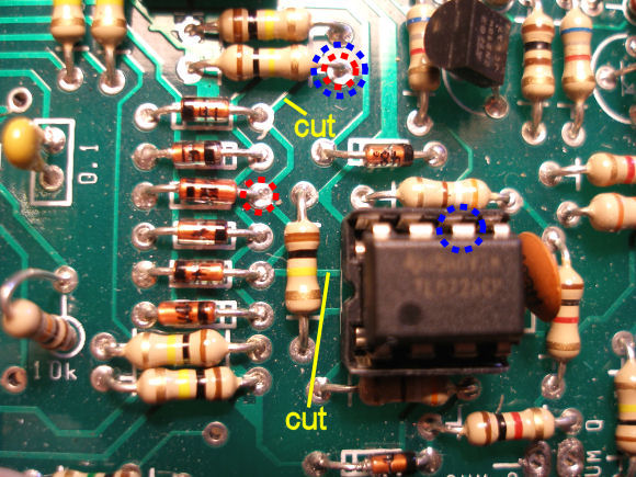
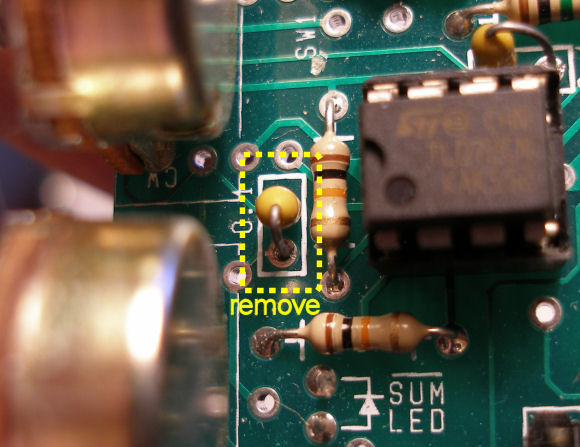
Also in the above: blue trace 1 is an offset triangle wave input from an LFO; traces 2, 3 and 4 are the gate outputs 'A', 'B' and 'C' respectively; trace 6 is the 'sum not' output 'A+B+C'. (Also note the middle 'sum' output pulse is narrower than the other two: this is due to an incorrect capacitor value inserted at build time, and is covered below.) The problem is due to a design flaw in the circuit: the edges are detected and summed by an arrangement of capacitors and diodes, and this is causing the input of the op amp which generates the pulses to go below the negative supply rail, and this is causing the op amp to misbehave—the end result being the narrow spikes in the 'sum' output. The solution is to introduce a resistor which reduces the size of the voltage (it is a bit of a 'hack', but seems to work well enough). Disassembling the module is easy enough, but care needs to be exercised as it is rather flimsy, due to the long lever-effect of the board sticking out, with only the three pots' mounting lugs trying to hold the PCB perpendicular to the faceplate. It is also probably easier to work with if the flying leads to the 'sum' out sockets are de-soldered at the board end, rather than undoing the sockets and having them flailing about the place! Locate this central part of the PCB, and cut the two tracks as indicated; underneath we solder a 47kΩ resistor between red points, and a wire link between the blue points:
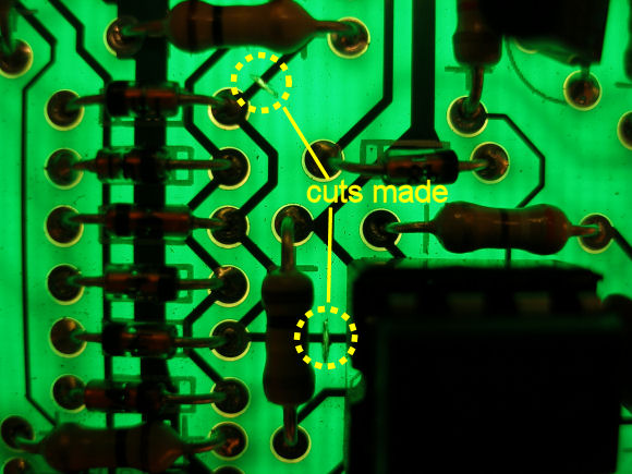
The following reinforces the locations of the cuts, and shows they do break the track (holding the PCB up to a light):
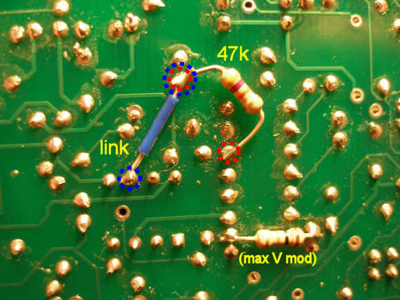
On the underside, solder a 47kΩ resistor between the two red points, and a wire link between the blue points:
That is all there is to it, so then carefully re-assemble the module (depending on whether any other changes are needed/required). This set of traces shows the spikes on the 'sum' out are no more (the trace descriptions are as before):
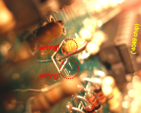
In the very first set of traces above the middle 'runt' pulse on my module was caused by an incorrect value capacitor having been fitted: the silkscreen is incorrect and calls for a 0.1μF (= 100nF = '104') cap; I actually had an '821' fitted (= 820pF ≈1nF); the correct value should be 10nF (= '103')—of course I changed it, and it can be seen in the traces immediately above that the pulse is now the same length as the other two:
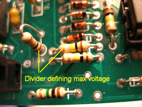
I fear there is thus a very good chance that others will have an incorrect value cap fitted in this location! Maximum threshold voltage modificationThe maximum threshold level which may be set by the pots (i.e. when they are fully clockwise) is defined by a simple resistive divider, which is then buffered by an op amp voltage follower and applied to the top of the pots. It appears the factory values of the divider are 10kΩ:100kΩ, giving 12×100/110=10.8V as the maximum voltage:
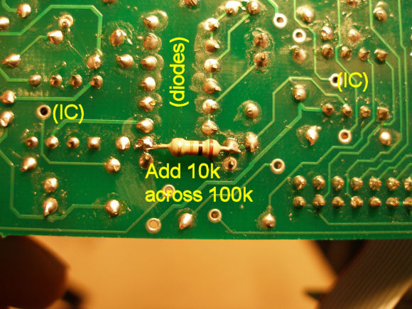
Some feel this wastes a lot of the pot usable travel when smaller signals are input to the module—many LFOs and envelope generators only go up to about 5V or so. Thus changing the resistor values allows us to change this maximum threshold level. As a simple solution, soldering another 10kΩ across the lower of the resistors, the 100kΩ, gives a max threshold of about 5.7V:
Unfortunately there is capacitor on the buffer output, which looks like it is meant to be a smoothing cap—with the change of voltage level due to the extra resistor, the buffer oscillates wildly, at about 480kHz. The cap really ought to be on the resistive divider on the buffer input in any case, so I simply removed it:
Here are the gates output for the minimum and maximum pot settings, with an approximately 6.5V signal input—the levels at which the gates switch are where the blue and (extended) green traces cut the red one:
If you want slightly more or less, change one or both resistors to suit! First law of CMOS violationWhilst filing some of my notes on this module I spotted that I had noted that the module design apparently breaks one of the basic commandments of CMOS, 'thou shalt not leave unused CMOS inputs floating'. Only three of the six sections in the '4049 hex inverter chip are used, and the inputs of the three unused sections, pins 3, 5 and 7, do not appear to be tied to either ground or the supply rail. Thus if you have a module that seems to be misbehaving in an odd way, then snaking a wire down these pins, from either pin 8 (ground), or pin 1 (+12V) may be worth trying! [Page last updated: 03 Feb 2011] |