![]()
|
|
Personal web pages ofTim Stinchcombe |
LMF100 Switched-Capacitor Filter
Update Summer 2011: shortly after this year's Synth DIY meet in Cambridge I realized I could easily add highpass and bandpass (12dB+12dB) options to this filter—once I can find a decent amount of vacation time, I fully intend to commit my ideas to a proper PCB... [I've not quite had the time to get everything ready to complete this page, but since the bulk of it is done, I thought I'd put it up without waiting.] A recurring topic on the Synth DIY list is whether any of the switched capacitor filter chips which are about are of any use when it comes to making filters for use in synthesizers. Whilst several people have reported less-than-inspiring results, I wanted to see for myself, so a few years ago I played around with one: the results, whilst being far from spectacular, were enough to make me build a complete filter, if only from the point of view of showing that it can reasonably be done. (But that being said, if you are expecting a low parts-count filter, you'd better look elsewhere!) Others appear to have mainly stuck to the circuits shown on the datasheets/application notes, which maybe accounts for the disappointing results. Most of the chips that I have seen seem to be based around the standard second-order state-variable set-up, and so there is limited scope with what can be done for higher-order filters. However it occurred to me that it might be possible to 'emulate' the standard four-pole filter \[H(s)=\frac{1}{(s+1)^4+k}\]which we all know and love (and possible hate for its all-pervasiveness!) from the likes of the Moog ladder, and chips such as the CEM3320, SSM2040 etc. My idea was to re-arrange the transfer function as \[H(s)=\frac{1}{(s^2+2s+1)^2+k},\]and see if I could implement each of the second-order expressions with one section of an MF10 chip (later I was more or less forced to change to using an LMF100, for reasons given below; links to datasheets etc. are at the bottom of the page). After some rather tedious calculations for all the resistor values concerned, I decided this was possible, and promptly breadboarded the circuit. (I should say that I have no idea what the filter would have sounded like using any of the example component values for the standard set-ups given in the datasheets, as I did not try them—I simply reasoned that since we know the standard four-pole filter given above is known to sound OK, that is what I would aim for.) It went through several revisions in order to get the gain structure right so that it would self-resonate at a high resonance setting, but the 'core' of the filter that I finally ended up with was this: 
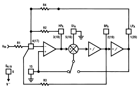
This shows the 'internals' of the LMF100 (with the '\(1/s\)' being the integrators of course), rather than just a pin-out, as I find this easier to read and understand; the numbers at some nodes are the actual pin numbers of the chip though. The configuration of the LMF100 follows 'Mode 3' of the datasheet and application note AN-307, and for the second section I have given the resistors the same designators, for ease of reference. The next section derives the transfer function. Transfer Function and Resistor SelectionHere is the 'Mode 3' configuration taken from Figure 11 of the datsheet:
Taking each of the integrators to be \(1/(\tau s)\), where \(\tau\) is the time-constant of the integrator, and annotating in the obvious way, we readily get \[V_{lp}=\frac{V_{bp}}{\tau s};\quad V_{bp}=\frac{V_{hp}}{\tau s};\quad V_{hp}=-R_2\left(\frac{V_{in}}{R_1}+\frac{V_{bp}}{R_3}+\frac{V_{lp}}{R_4}\right),\]which are easily manipulated into \[\frac{V_{lp}}{V_{in}}=\frac{\displaystyle-\frac{R_2}{R_1}}{\displaystyle\tau^2s^2+\frac{R_2}{R_3}\tau s+\frac{R_2}{R_4}},\]and then into \[\frac{V_{lp}}{V_{in}}=\frac{\displaystyle-\frac{R_4}{R_1}}{\displaystyle\frac{R_4}{R_2}\tau^2s^2+\frac{R_4}{R_3}\tau s+1},\]by factoring to get the constant equal to \(1\) in the denominator. Now substitute for \[\omega_c=\frac{1}{\tau}\sqrt{\frac{R_2}{R_4}},\]to get \[\frac{V_{lp}}{V_{in}}=\frac{\displaystyle-\frac{R_4}{R_1}}{\displaystyle\frac{s^2}{\omega_c^2}+\frac{R_4}{R_3}\sqrt{\frac{R_2}{R_4}}\frac{s}{\omega_c} +1},\]from which we can see the lowpass gain is \(-R_4/R_1\) and \[Q=\frac{R_3}{R_4}\sqrt{\frac{R_4}{R_2}}=\frac{R_3}{R_2}\sqrt{\frac{R_2}{R_4}},\]both of which agree with the corresponding quantities in the datasheet (p15); we are also given \[f_0=\frac{f_{clk}}{100}\sqrt{\frac{R_2}{R_4}}\equiv f_c,\](for pin 12 at mid-rail), and from above we get \[f_c=\frac{1}{2\pi\tau}\sqrt{\frac{R_2}{R_4}},\]and so we can then deduce that \[\tau=\frac{100}{2\pi f_{clk}}\equiv\frac{100}{\omega_{clk}}.\]For simplicity I chose to make \(R_1=R_4\), so the gain of each section is \(1\) (the minus signs of each section cancel); I also wanted to keep the clock frequency out of the audible range, if at all possible, and after much juggling of numbers concluded that a \(400:1\) ratio of clock to cut-off frequency was achievable, both in terms of practical resistor values, but also whatever circuitry generates the clock itself, and hence I made \(R_4=16\times R_2\), so \(f_c=f_{clk}/400\). I then picked \(R_2=10\text{k}\Omega\), so \(R_1=R_4=160\text{k}\Omega\), and taking \(R_3\) as \(20\text{k}\Omega\) gives the \(s\) coefficient as the desired '\(2\)': \[\frac{R_4}{R_3}\sqrt{\frac{R_2}{R_4}}=\frac{160}{20}\sqrt{\frac{10}{160}}=2.\]At the time I obviously didn't check to see if 160kΩ was a preferred value or not, as I simply used 150kΩs instead: this makes the denominator of each section \[s^2+1.936s+1,\]which I'm not particularly bothered about.
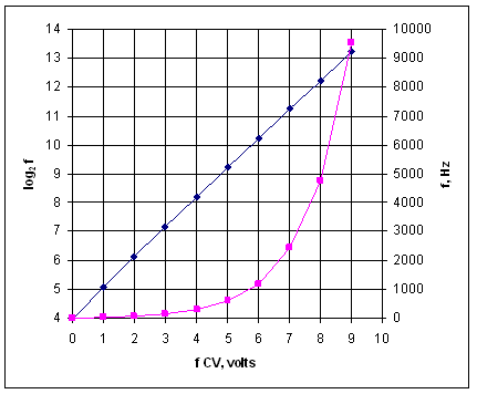
variable gain \(k\) in the feedback loop (via the one OTA section); and a subtractor (from the second OTA section, at fixed gain), subtracting the feedback from the input before being applied to the first filter section. Thus it is straightforward to show that the overall transfer function is (approximately) the desired \[H(s)=\frac{1}{(s^2+2s+1)^2+k}.\]SchematicsBefore going into further minutiae of the design, here is a pdf of the schematics. [When I got about half way through this lot, it occurred to me that it was turning into something of a switched-capacitor filter design tutorial, but so be it!] Gain RegimeI wanted voltage-control of the resonance, up to self-oscillation, thus requiring k=0 to 4 (ish) in the feedback path, and so an operational transconductance amplifier (OTA) seemed like the natural choice; the feedback needs subtracting from the input, and using the second section from an LM13700 thus seemed an obvious thing to do (CA3080s would do just as well, but then it would seem wasteful using a second one merely as a fixed-gain amplifier, as is done here). The current output from the subtractor can directly feed the 'virtual ground' (actually mid-rail) of the first filter section, thus doing the job of its 'R1' resistor: the standard equation for current out of an OTA is Vdiff×19.2×Iabc, where Vdiff is the differential input voltage, and Iabc the amplifier bias current; the input Vin is attenuated by about a 1/200th to keep the OTA operating aproximately in its linear region; hence we want (Vin/200)×19.2×Iabc to look like Vin/150k; equating and re-arranging these gives an Iabc of about 70μA, which is readily achieved with the 150kΩ resistor from the 12V rail to the Iabc pin. Use a similar argument to derive the required Iabc of the feedback OTA which will give a max gain of 4×Vout around the loop: 4Vout/150k=(Vout/200)×19.2×Iabc×300×19.2×70μ, which when re-arranged gives an Iabc of about 690μA for a gain of 4, comfortably in the range of the Iabc for an OTA. (And for those still paying attention, I leave it as an exercise to speculate on the suitability, in terms of the linearity of the OTA, of the choice of 300Ω for the resistor at the inverting input the second OTA...) Clocking/Cut-Off Frequency ControlThe idea of making the clock to cut-off frequency ratio about 400:1, to minimize the range over which the clock can be heard, is not without consequences (recall, pin 12 of the LMF100 at mid-rail gives 100:1; this is then multiplied by the square-root of R4/R2, ≈ 4, giving the 400:1). If we say 16kHz is the limit of hearing, then in theory we can get the cut-off frequency down to about 16,000/400 = 40Hz before we can hear the clock, and this seems like a useful value. However, at the other end, a maximum cut-off of 10kHz would require a clock speed of 400×10,000 = 4MHz: I was originally looking at using the MF10 chip for this filter, but I felt it was rather restrictive with respect to this requirement, as its specified maximum clock frequency of 1.5MHz would result in a maximum cut-off frequency of only 3.75kHz. Fortunately its higher-spec'd sibling, the LMF100, comes to the rescue, as its maximum clock frequency is given as typically 3.5MHz, giving a maximum cut-off frequency for the filter as just below 9kHz, which I see as much more acceptable. The VCO in a '4046 PLL chip supposedly shows good linearity with the applied control voltage, and so I decided to use one of those. However I then discovered that not all 4046s are equal: the standard '4000' series HEF4046 only has a specified centre frequency of 2.7MHz (at 15V), yet I wanted to go up to around 3.5-4MHz; fortunately more modern technologies come to the rescue, and I have used a TI CD74HCT7046 which has a specified minimum center frequency of 12MHz, ample for the filter's needs (but this is at 5V, and so a source of 5V was going to have be designed into the circuit as well—fortunately the LMF100 is happy with a 5V clock, despite being run off 12V itself). I also learnt it was possible to drive the 4046 VCO with a current sink at pin 12. I thus used the fairly standard PNP-NPN exponential converter set-up, sinking current from that pin, and it seems to perform well enough (see the chart below). The resistor R50 at pin 12 is to limit the maximum clock speed (by forcing the transistor to saturate), as the filter chip gets real nasty if clocked too fast! (And for the 4046 timing cap I found what looks to be an old polystyrene type.) Other points of note:In order to emulate a 'reverse log' type of law for the resonance control, to stop the resonance 'coming in all at once', I used a diode in parallel with a resistor in the feedback of an op amp (D1/R18)—the value of the resistor could be altered to give a different shape, if required. The voltage then needs converting to a current to feed the OTAs, and the crude current-mirror approach is used to avoid running into problems of hitting the voltage rail. DC offsets were a problem with my initial experiments whilst using the MF10: they accumulate around the circuit, and are exacerbated by using the large resistor values to push up the clock ratio; for the MF10 they are given typically as 140mV, and under some circumstances were so large as to restrict the signal swing; this was another reason for switching to the LMF100, for which, thankfully, the offsets are an order of magnitude smaller, being given as ±15mV; in addition, for the final version I incorporated trimpots to hopefully minimize their impact, R31 and R49 (and R17 and R21 are there for good measure to counter any imbalance in the OTA input stages—in any case, I didn't use any special set-up method, merely set the filter oscillating, and twiddled each pot to check the signal was as close around mid-rail as I could get it!). Apart from PL6 which is a 10-way header, the other PLXs in the schematic were just an expedient for 'tagging' points on the PCB at which to attach flying leads which actually went to the appropriate sockets. The two chokes L1 & L2 are just there as insurance to hopefully prevent any clocking noise getting back into the ±12V supply rails. PerformanceThe following chart shows the variation in (cut-off) frequency versus the applied control voltage. The mauve trace against the right-hand axis is the actual frequency of the filter self-oscillating, and runs from 16Hz at 0V in to about 9.5kHz at 9V in; the blue trace, against the left-hand axis, is log2f, whose near '1-in-1' gradient shows that it is pretty close to being 1V/octave:
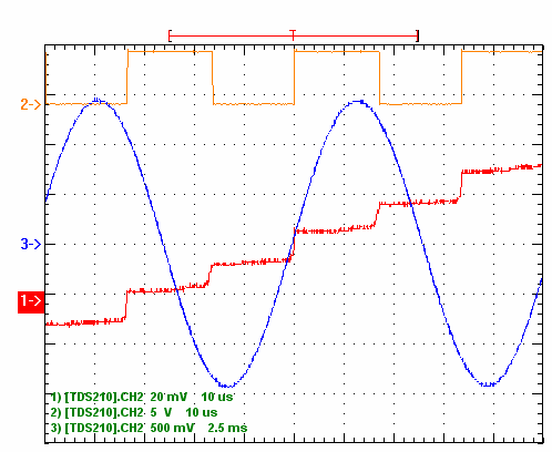
Averaging the frequency of oscillation to the clock gives a ratio of 388:1, i.e. close to the 400:1 design aim, so the clock is running from just above 6kHz to around 3.6MHz. For the following (combined) scope shot the filter was set to oscillate at around 80Hz (blue trace—be aware of the different vertical and horizontal scales!), showing a nice sine-shape; expanding the timebase we can eventually see the actual steps in the waveform caused by the discrete switching action (red trace); for comparison with the stepped-waveform, the actual clock output, running at around 31kHz, is also given (orange trace):
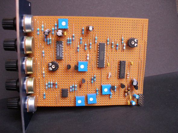
[Hopefully some Bode plots to follow too.] Sound samplesHere is an On the Run-type sequence, with LFOs slowly modulating both the cut-off frequency and the resonance. Here is a really simple sample, where the clock noise can be heard; a low frequency square-wave is input to the filter, and the cut-off is modulated by a slow-running LFO; resonance is set to zero. The frequency knob is set at a frequency above the input signal, but the LFO voltage is sweeping the filter well above and below this (by approx. ±5.5V); thus in the 'trough', the cut-off is just a few Hz, and the 'sizzle' of the clock frequency, at a minimum of around 1.7kHz, can just be heard. ConstructionI couldn't be bothered to layout a proper PCB, so I simply used stripboard—the following photo shows the result:
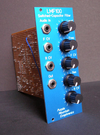
I got the front panel made by the excellent Schaeffer AG, using their Front Panel Designer software. Texas Instruments LMF100 & MF10 linksLinks to the Texas Instruments website: LMF100: overview page; and datasheet. (Texas Instruments acquired National Semiconductor in 2011.) [Page last updated: 17 Dec 2022] |